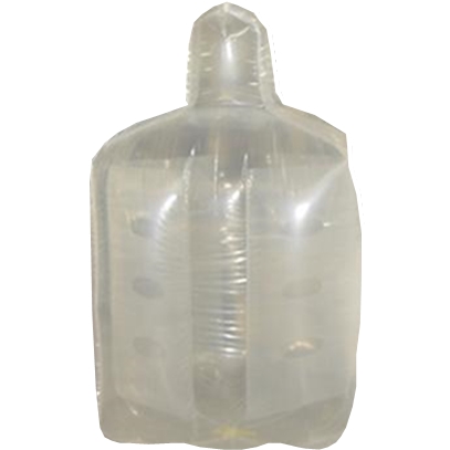
Multilayer co-extruded conductive bag
The charged carriers of the conductive film are scattered by the surface and the interface during the transport process. When the thickness of the film can be compared with the free path of electrons, the influence on the surface and the interface will become significant. This phenomenon is called thin film. size effect. It is equivalent to the reduction of the free path of the carriers, and thus the conductivity of the film is smaller compared to the bulk of the same material. Due to the imperfect preparation technology, the defect concentration in the film is usually relatively high, and the main defects are impurities, vacancies, interstitial atoms, dislocations, grain boundaries, and adsorption and segregation at the surface and interface.
